Part of the SPIE Conference on
Surface Characterization for Computer Disks,
Wafers, and Flat Panel Displays San Jose,
California January 1999
Proceedings of SPIE pp.53-64
MR Glide Inspection for Hard Disk Defect Detection
Michael Boyd and Xiaopeng Xu
Phase Metrics, Inc., Fremont, California
ABSTRACT
In a disk drive magnetic read/write is achieved with a magnetic head flying closely over a magnetic disk. As area1 recording density is increased to several Gbits/In2, the dynamic flying height of the magnetic head is reduced to one m-inch or less. Bumps taller than one m-inch often results in head crash. Since the DLC coating on the magnetic disk surface is less than 10 nanometers in thickness, pits with depth over 10 nanometers cause damage to the magnetic layer. To prevent head crash or missing bit errors, magnetic disk surface needs to be examined for bumps taller than the dynamic flying height and pits deeper than the DLC thickness. In this paper, we report experimental results using a head with an MR sensor flying over a disk with precision bumps and pits micro-fabricated on the disk surface. Non-contact signal disturbances of the MR sensor flown over variable area square pits and bumps on the 2400 Oe media exhibit both magnetic and thermal signal characteristics. The lateral sizes of the pits and bumps obtained using the MR magnetic signal measured from a Phase Metrics MG250 tester agree well with those measured with an Atomic Force Microscope (AFM). The thermal signal characteristics of the pits and bumps are of opposite polarity, and scale in a non-linear fashion with the lateral size of the surface defects. Some preliminary experimental results involving naturally occurring surface defects and Phase Metrics' optical scatterometry tester PS5100 are also discussed for comparison purposes.
Keywords: MR Glide, MR thermal signal, MR magnetic signals, scatterometry, specular light, bright field, scattered light, dark field, Atomic Force Microscope, Magnetic Force Microscope, Magnetic Phase Microscope
1. INTRODUCTION
1.1 High density recording requires that the hard disk surface be free of defects as small as 1mm x 1mm in areal size or less. Current methods for characterizing defects of this size are limited to a slow metrology technique such as Atomic Force Microscopy (AFM), and associated Magnetic Force Microscopy (MFM) and Magnetic Phase Microscope (MPM). An AFM micro-image from a 10mm x 10mm area pit (2 m’’ in depth) is shown in Figure 1. Faster defect detection techniques utilize a spin stand such as magnetic certification testers that detect missing pulses with high frequency write and read (i.e. Phase Metrics MG250), or Optical Scatterometry testers that detect surface defects using bright and dark field signals (i.e. Phase Metrics PS5100). A certification missing pulse signal and an optic bright/dark field signal for the same 10mm x 10mm area pit are also shown in Figure 1.
1.2 In this study we explore the possibility of using the magnetically biased MR element in current recording heads to detect defects and characterize them by type and length along the track circumference direction without high frequency read/write. Previous work has focused on contact type thermal asperity detection (the MR thermal signals from large natural or manufactured defects). This paper demonstrates that the responses of the magnetically biased MR elements from defects on a DC erased disk contain both the magnetic signals and the thermal signals, as shown in Figure 1, and these signals can be utilized to characterize small pits and bumps.
1.3 For a typical SAL MR head, the change in modulation voltage is dependent on the bias field, the temperature field and the media magnetization[1][2]. The dependence on media magnetization was examined by DC erasing the media in opposite directions. The dependence on bias field and the temperature field was studied by applying various bias currents. Most of the results reported were taken from micro-fabricated defects and some data taken from naturally occurring defects are also presented. For comparison purposes optical signals recorded from a Phase Metrics PS5100 optical scatterometer are shown for both manufactured and naturally occurring defects.
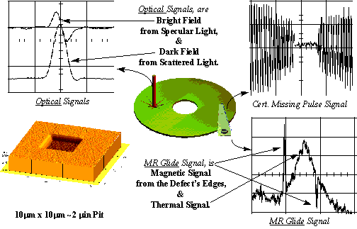
Figure 1. MR Glide, Missing Pulse and Optical Signals for a 10 mm x 10 mm pit
2. METHODS
2.1 Fourteen defects were fabricated on a 2400 Oe 31.5mil 95mm MR disk using a Focused Ion Beam (FIB) . Seven ~1.25 min height bumps were deposited, and seven ~2uin deep pits were etched, on the disk 50 mils apart along a radius. The specified dimensions were 40mm x 40mm, 20mm x 20mm, 10mm x 10mm, 6mm x 6mm, 4mm x 4mm, 2mm x 2mm, and 1mm x 1mm respectively. The disk was mounted on a Phase Metrics MG250 certifier and DC erased using a 50% thin film inductive write head. The MG250 read channel was then used with an MR head containing a Soft Adjacent Layer (SAL). The MR bias current was at 16mA, and the linear velocity was maintained at 500 ips. The MR head was moved to the approximate location of the defect under analysis, and then stepped on a radius until an MR thermal signal was detected on a Lecroy Oscilloscope. The signal was optimized for maximum signal level. The maximum signal measured was recorded and characterized for both MR modulation and thermal signal amplitude and timing characteristics.
2.2 After the MR glide inspection, the disk was removed from the certifier and mounted on a Park Scientific AFM. Each individual defect was characterized utilizing the Park Scientific AFM for defect width along the direction of the circumference. With an MFM cantilever, the defect was scanned for its AFM, MFM, and MPM images. The MFM cantilever tip had zero bias applied to it during data acquisition. The resulting magnetic phase images were then compared to the MR read head signal recorded for this defect. To examine the effect of erase polarity on the MG glide signals, the two wire connected to the write transducer were disconnected, and re-attached to the head paddle board for the opposite polarity to be applied to the write element during DC erasure. The inductive head was again set to a 35mA constant erase current, and the resulting MR element read back signal was recorded at 16mA, and 500 ips, using the Lecroy scope.
2.3 To examine the effect of the MR bias current on the MR glide signals, various bias currents were used while other testing conditions remained the same. The MR element read back signal was recorded using the Lecroy scope with bias current varying from 3mA to 18mA, at 1mA steps. The resulting Lecroy image was characterized for MR modulation signal , and thermal signal amplitude, as a function of MR bias.
2.4 For comparison purposes, the same disk containing the fourteen fabricated defects was placed on a Phase Metrics PS5100 optical scatterometry tester. Figure 2 provide an overview of the PS5100 optical heads design. The optical head was moved to the approximate location of the defect under analysis, and then stepped on a radius until the maximum optical signals were observed and recorded on a Lecroy
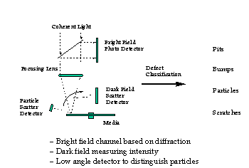
Figure 2. Optical Inspection System Overview
Oscilloscope. A disk containing naturally occurring defects was also inspected using MR glide on the MG250 and optical scatterometry on the PS5100. The MR Glide signals for three different type defects were recorded and characterized on a Lecroy Oscilloscope and compared with these obtained from PS5100.
3. RESULTS
3.1 Each defect was characterized for defect geometry using an AFM. The AFM measured defect width and height (or depth), along with its MR modulation signal characteristics, and thermal signal characteristics, are listed in Table 1. Once the MR glide inspection was performed on each defect, the signals were analyzed for magnetic, thermal and timing characteristics. Figure 3 shows the AFM Micrograph and MR Signal from a 6mm x 6um Pit with ~ 7.2nm Steps. Notice that the MR signal contains both the thermal base line modulation and the magnetic spikes. The small step around many of the defects was created as an artifact of the FIB fabrication process. This small step, on the order of 7nm (or 1/4min) induced an MR modulation signal but not the thermal signal. This demonstrates the MR modulation sensitivity to sub-microinch defects. The distance from the edge of the pit to the step was equivalent to the distance calculated utilizing the time delay between the corresponding spikes times the linear velocity. The results are listed in Table 1. A graph of the calculated width as a function of the measured AFM width for all pits and bumps is shown in Figure 4. The graph demonstrates a nearly perfect correlation between AFM measured width and the calculated one. A perfect correlation would have a slope of one and correlation coefficient of one.
|
Design |
Defect |
AFM |
AFM Height |
MR Modulation |
MR Modulation |
Thermal Signal |
Thermal Signal |
|
Width (mm) |
Type |
Width (mm) |
or Depth (min) |
Pulse Delay(mSec) |
Delay x . Velocity(mm) |
Maximum Ampl(Vp) |
Minimum Ampl(Vp) |
|
40 |
Bump |
40.9 |
1.27 |
3.23 |
41.021 |
NA |
-2 |
|
20 |
Bump |
20.2 |
1.22 |
1.6 |
20.3 |
NA |
-0.805 |
|
10 |
Bump |
10.9 |
1.27 |
0.858 |
10.8966 |
NA |
-0.304 |
|
6 |
Bump |
6.56 |
1.22 |
0.518 |
6.5786 |
NA |
-0.185 |
|
4 |
Bump |
4.76 |
1.24 |
0.38 |
4.826 |
NA |
-0.14 |
|
2 |
Bump |
2.8 |
1.04 |
0.218 |
2.7686 |
NA |
-0.065 |
|
1 |
Bump |
2.4 |
1.05 |
0.19 |
2.413 |
NA |
-0.04 |
|
40 |
Pit |
42.2 |
1.7 |
3.31 |
42.037 |
0.378 |
NA |
|
20 |
Pit |
20.4 |
1.99 |
1.59 |
20.193 |
0.287 |
NA |
|
10 |
Pit |
10.3 |
2.02 |
0.814 |
10.3378 |
0.245 |
NA |
|
6 |
Pit |
6.28 |
1.92 |
0.498 |
6.3246 |
0.163 |
NA |
|
4 |
Pit |
4.25 |
1.59 |
0.34 |
4.318 |
0.141 |
NA |
|
2 |
Pit |
2.4 |
1.65 |
0.208 |
2.6416 |
0.102 |
NA |
|
1 |
Pit |
1.28 |
1.86 |
0.104 |
1.3208 |
0.055 |
NA |
Table 1 measured geometric, MR Modulation Signal, and Thermal Signal parameters
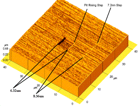
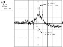
Figure 3. AFM Micrograph and MR Signal from a 6mm x 6um Pit with ~ 7.2nm Steps
3.2 The characteristics of MR glide thermal signals.
3.2.1 In Figure 5 and 6, the AFM micro-graphs and the MR read signals are shown for a ~1mm x 1mm 1.8uin deep pit and a ~20mm x 20mm 1.22min High Bump respectively. Apparently, the signal amplitude, width and polarity depends on the size and the type of the defects. It was noted that the thermal signal of bump defects exhibited a negative polarity pulse as shown in Figure 3, which decreased in amplitude with decreasing defect width. The thermal signal of pit defects exhibited a positive polarity pulse as shown in Figure 5, which also decreased in amplitude with decreasing defect width.
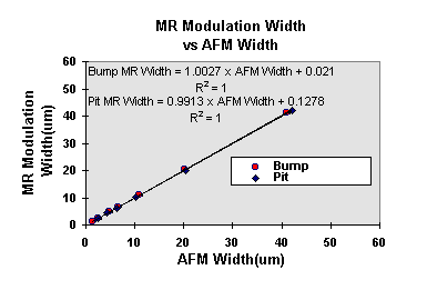
Figure 4. MR Modulation Signal Width times Linear Velocity vs AFM Width
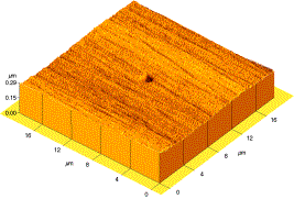
Figure 5. AFM Micrograph and MR Signal from a ~1mm x 1mm 1.8uin Deep Pit
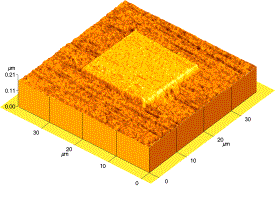
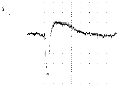
Figure 6. AFM Micrograph and MR Signal from a ~20mm x 20mm 1.22min High Bump
3.2.2 The bump MR thermal signal was graphed as a function of negative amplitude in Figure 7. The bump thermal signal increased non-linearly with increasing defect width.
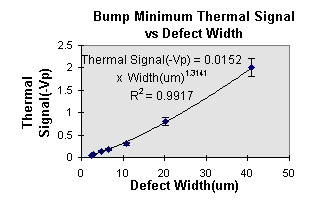
Figure 7. Bump Thermal Signal Increases with Defect Width
3.2.3 The pit MR thermal signal was graphed as a function of positive amplitude in Figure 8. The pit thermal signal also increased non-linearly with increasing defect width.
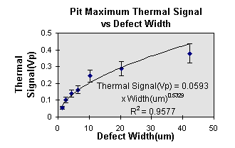
Figure 8. Pit Thermal Signal Increases with Defect Width
3.3 The Characteristics of MR glide magnetic signals.
3.3.1 Using a Park Scientific AFM with an MFM cantilever, a 10mm x 10mm area pit was scanned for its AFM, MFM, and MPM images. The AFM micrograph cross section images and the associated depth profile are displayed in Figure 9. The MFM micrograph cross section image, and the associated magnetic force profile is displayed in Figure 10. The MPM micrograph cross section image, and the associated magnetic phase profile is displayed in Figure 11. The MR element read signal from the 10mm x10mm area pit is displayed in Figure 12 . Notice the remarkable similarity of the MR read signal displayed in Figure 11 with the magnetic phase profile displayed in Figure 10.
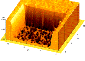
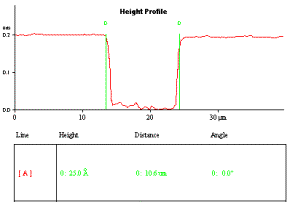
Figure 9 AFM Micrograph Cross Section , & Profile of a 10mm x 10mm Pit
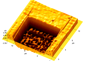
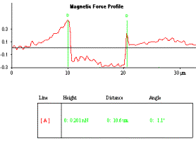
Figure 10 MFM Micrograph Cross Section , & Profile of a 10mm x 10mm Pit
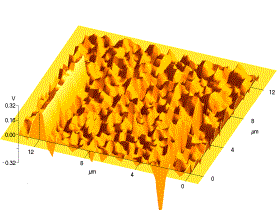
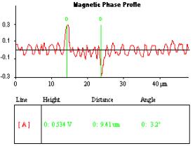
Figure 11 Magnetic Phase Micrograph Cross Section , & Profile of a 10mm x 10mm Pit
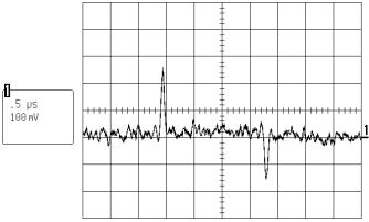
Figure 12 MR Element Read Signal @10mA Bias & 500 ips
3.3.2 To examine the dependence of MR glide on DC erase polarity, the two wire connected to the write transducer were disconnected, and re-attached to the head paddle board for the opposite polarity to be applied to the write element during erasure. The resulting signals are recorded in Figure 13. The MR magnetic modulation signal pulses flipped polarity as expected. The MR thermal signal polarity remained the same, independent of the erase polarity of the media. The associated signal amplitude did not show symmetry with change in erase direction.
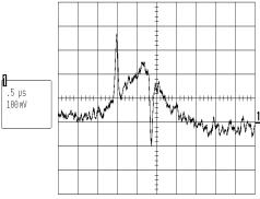
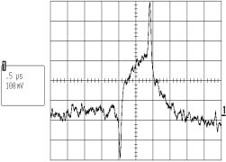
Figure 13. MR Signals at 16mA and 500 ips with opposite polarity erase on a MR disk
3.3.3 The dependence of MR glide signals on MR bias current were examined by varying the bias current scope from 3mA to 18mA, at 1mA steps. The MR signal for the same 10mm x 10mm area pit is shown in Figure 14. Notice the differences between Figure 12 and 14. The modulation maximum amplitude plus the thermal signal amplitude, and minimum amplitude plus the thermal signal amplitude, is plotted as a function of MR bias current in Figure 15. The thermal signal as a function of MR bias current is plotted in Figure 16. For this 10mm x 10mm area pit no thermal signal was observed below 8mA bias current.
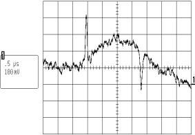
Figure 14. MR Read Signal at 10mA, and 18mA MR bias current.
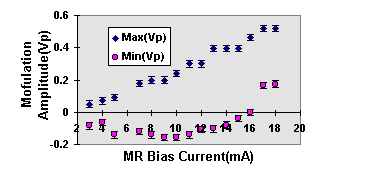
Figure 15 MR Read Head Modulation Signal vs. MR Bias Current
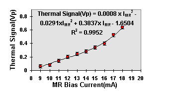
Figure 16 MR Read Head Thermal Signal vs. MR Bias Current
3.4 Comparison of MR Glide to PS5100 Optical Signal from Natural Defects.
3.4.1 A disk containing naturally occurring defects was placed on the MG250 and the MR Glide signal for different types of defects was recorded on a Lecroy Oscilloscope. The same disk was then placed on the PS5100 and the defects were characterized for their optical signals photo images. Figure 17 exhibits the results from a scratch type defect on the disk’s surface. The PS5100 optical signal exhibit dark field signal from scattered light only, and the MR Glide signal exhibits magnetic transition pulses only, with no thermal signal present. Figure 18 exhibits the results from a shallow pit type defect on the disk surface. The PS5100 optical signal exhibit bright field signal from specular light only with the characteristic signal polarity of a pit. The MR Glide signal exhibits thermal signal only, with little magnetic transition signals present, but the characteristic polarity thermal signal of a pit. The lack of sharp transition edges on the defect precludes the detection of optical dark field signal from scattered light, and MR Glide magnetic transition pulses from the defects edges. Figure 19 exhibits the results from a short bump type defect on the disk’s surface. The PS5100 optical signal exhibit bright field signal from specular light only with the characteristic signal polarity of a bump. The MR Glide signal exhibits mostly thermal signal, with little magnetic transition signals present, but the characteristic polarity thermal signal of a bump.
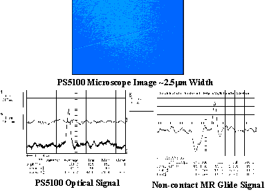
Figure 17 Photograph with Optical Signals and MR Glide Signal from a Scratch

Figure 18 Photograph with Optical Signals and MR Glide Signal from a Pit
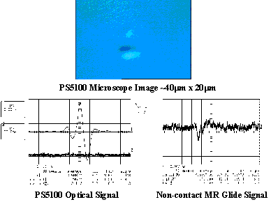
Figure 19 Photograph with Optical Signals and MR Glide Signal from a Bump
3.4.2 It should be noted that for some large defects we tested we saw the large thermal signal dominates the MR modulation signal. The flash temperature rise (or drop) nearby the MR sensor due to head disk contact leads to a thermally induced signal from the MR read element [3,4]. This is called a “thermal asperity”, and this effect is not examined in this article. As the MR element flies near contact with the surface, the disk waviness induces a signal from the MR sensor[5]. When a bias current is applied to the MR element, its temperature will rise due to the Joule heating effect. The temperature rise DT can be calculated from a measurement of resistance change of the MR element DR by the relationship; DT=DR/(aRo), where the Ro and a are the initial resistance and the temperature coefficient of the MR element. In an SAL based MR head, (as was used in this experiment), there is a linear relationship between DT and DR (within a range of bias currents). The increase in the MR (non-contact pit thermal) signal corresponds to the increase in the spacing, while the big drop in the MR (non-contact bump thermal) signal corresponds to the decrease in spacing[6], as was exhibited with the defects in this article. In Figure 3 we see the increased signal from the baseline resulting from an increase in spacing between the disk and MR element, and in Figure 6 we see the decreased signal from the baseline resulting from a decrease in spacing between the disk and MR element .
4. CONCLUDING REMARKS
4.1 An MR element flying over DC erased media can be used to detect micro-fabricated pit and bump defects down to the 1mm x 1mm in area and to less than 1m” height/depth. The MR modulation signal corresponds to the switch in the magnetization polarity of the media[7]. The product of the time change between the positive and negative magnetic transition modulation pulses times the linear velocity scales to within 200nm of the defects width along the circumference as measured with an AFM. The MR element experiences increasing thermal signal with increasing defect size. Pit defects exhibit a positive going thermal pulse on the MR signal representing decreased heat dissipation due to increased MR element and disk spacing. Bump defects exhibit a negative going thermal pulse on the MR signal representing increased heat dissipation due to a decrease in the MR element and disk spacing. The MR magnetic modulation signal induced by a micro-fabricated defect is dependent on the polarity of DC erase on the MR media but the MR thermal signal is independent of the polarity of DC erase. The non-contact MR thermal signal is IMR3 dependent on the applied MR bias current. The preliminary MR Glide signals from naturally occurring defects exhibit excellent agreement in classifying defects by type in comparison to Phase Metrics’ PS5100 optical scatterometer. The results found in this article demonstrate MR Glide as a very promising technique for hard disk surface inspection without using high frequency read/write.
ACKNOWLEDGMENTS
We would like to thank Gedeon Heinrich, Heiner Sussner, Blasius Brezoczky, George Burt, Dave Ferry, Veronica Munro, Brian-Tinh Vu, and Mike Rogowski for technical discussions and managerial support.
REFERENCES
[1]
H. N. Bertram, Theory of Magnetic
Recording, 1994
[2]
E. Sawatzky, Data Storage., Vol. 5,
No.3, p 49, 1998
[3]
R.D. Hemstead, IBM J. Res. & Dev., Vol. 18, p547, 1974
[4]
E. Schreck, R.E. Fontana, and G.P. Singh, IEEE
Trans. Mag., Vol. 28, p2548, 1992
[5]
M.M. Dovek, et al., U.S. Patent
5,455,730 1995
[6]
H. Tian, et al, IEEE Tans. Mag., Vol. 33, p3130, 1997
[7] G. Heinrich and X.-P. Xu, Phase Metrics Report, 1998